- +44 1480 464 066
- sales@orbitalfl.com
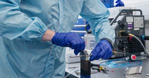
Advancements in electric vehicles, edge computing, and the growth of AI technology are driving the semiconductor market every day. Fabricating semiconductors involves incredibly precise processes, steps like photolithography, deposition, etching, ion implantation and diffusion, are all performed in ultra clean contaminate-free environments. This makes high purity gas and fluid handling systems not just important, but absolutely fundamental to ensuring high manufacturing yields.
Overview of Semiconductor Manufacturing
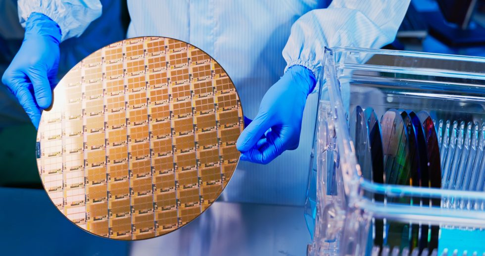
The manufacturing of semiconductors involves several critical stages, each playing a vital role in the development of the devices. It begins with Wafer Preparation, where silicon is refined and reshaped into ingots before being sliced into discs known as wafers. This stage is followed by a series of process steps; deposition, photolithography and etching, where a light sensitive photoresist is applied to the wafer. Unprotected areas of the wafer are etched away, creating nanoscopic structures essential for the circuit’s functionality. Stages of Ion Implantation and diffusion dope the material, where ions are introduced to areas of the wafer, altering its electrical properties to form functional semiconductor material.